Array
(
    [content] =>
    [params] => Array
        (
            [0] => /forum/index.php?threads/tsmc-phoneix-arizona-fab-construction-update.17955/
        )

    [addOns] => Array
        (
            [DL6/MLTP] => 13
            [Hampel/TimeZoneDebug] => 1000070
            [SV/ChangePostDate] => 2010200
            [SemiWiki/Newsletter] => 1000010
            [SemiWiki/WPMenu] => 1000010
            [SemiWiki/XPressExtend] => 1000010
            [ThemeHouse/XLink] => 1000970
            [ThemeHouse/XPress] => 1010570
            [XF] => 2021370
            [XFI] => 1050270
        )

    [wordpress] => /var/www/html
)
Guests have limited access.
Join our community today!
Join our community today!
You are currently viewing SemiWiki as a guest which gives you limited access to the site. To view blog comments and experience other SemiWiki features you must be a registered member. Registration is fast, simple, and absolutely free so please, join our community today!
You are using an out of date browser. It may not display this or other websites correctly.
You should upgrade or use an alternative browser.
You should upgrade or use an alternative browser.
TSMC Phoneix Arizona Fab Construction Update
- Thread starter hist78
- Start date
DaRAGingLunatic
Member
Wow its all massive there. Lots of work.
It doesn’t matter, but I must say I’m not a big fan of the architectural choices made. I think Fab18 and 12 have much nicer looking offices, I also think their shells look nicer too. Samsung has a very striking ascetic for their shells. Intel sites generally look a bit wonky given the ages, but NM/IR/the old joint Micron fab are my favorite intel sites from an ascetics perspective.
Mooredaddy
Well-known member
TSMC is very utilitarian in my estimation. Fits with their corporate culture lolIt doesn’t matter, but I must say I’m not a big fan of the architectural choices made. I think Fab18 and 12 have much nicer looking offices, I also think their shells look nicer too. Samsung has a very striking ascetic for their shells. Intel sites generally look a bit wonky given the ages, but NM/IR/the old joint Micron fab are my favorite intel sites from an ascetics perspective.
I have been through quite a few fabs in my 40 years and I have never been impressed by architectural choices. Seeing them via drone however is quite a different perspective. I am now duly impressed.
hist78
Well-known member
@hist78, thanks for sharing. I've been to many fabs but this is beyond impressive. Thrilled to see ever stronger US-Taiwan partnership!
You are welcome!
Some random thoughts:
1. I don't know what measuring system (metric vs English) Intel uses in its fabs. I assume for consistency, accuracy, and efficiency, TSMC will use as much metric system as possible in building construction, equipments, operations, and manufacturing.
2. A big portion of property tax in Arizona and Texas are used for K to 12 education. Hope TSMC will not demand local school districts to subside TSMC's fab projects. TSMC has an opportunity to show the world that they are different and they do care children's education.
3. The phase 2 of TSMC Phoneix Arizona fab seems progressing very well. It should be able to go live in 2026 as planned.
hist78
Well-known member
Feels like just yesterday they announced they were coming to Arizona, and now there’s a whole fab right there. Incredible.
Where’s the update videos for Intel Fab 52 & 62?
I found this one for Intel fab 52 but it's five months old.
hist78
Well-known member
Here is the update for the Intel Ohio fab construction:

 www.nbc4i.com

Intel to move into next phase of New Albany plant construction Tuesday
Watch recent NBC4 drone footage above to see progress on the Intel construction site as of March 2023. NEW ALBANY, Ohio (WCMH) — Intel is scheduled to shift into the next phase of constructio…
 www.nbc4i.com
See another article about TSMC's struggle to hire enough qualified people in Taiwan, they actually invest in educating high school students about semiconductors!2. A big portion of property tax in Arizona and Texas are used for K to 12 education. Hope TSMC will not demand local school districts to subside TSMC's fab projects. TSMC has an opportunity to show the world that they are different and they do care children's education.
Three years ago, TSMC announced its intention to invest billions to build a fab in Arizona. Since then, we have announced our further commitment to bringing the most advanced semiconductor manufacturing to the U.S., including the announcement that TSMC Arizona’s first fab would produce N4 process technology by 2024 and the announcement that we have started the construction of a second fab that would produce 3nm process technology by 2026. Our total investment in Arizona is now $40 billion, making TSMC’s investment the largest foreign direct investment in Arizona history. Phase 1 is on track and on schedule to start production in late 2024 and we are currently in the process of moving-in and installing tools—including EUV tools, deposition systems, and wafer cleaning tools—into the fab. When operational, this will be the most advanced chip-manufacturing process technology on U.S. soil and our customers will benefit from having the proximity of a world-class foundry and the supply chain that surrounds this industry.
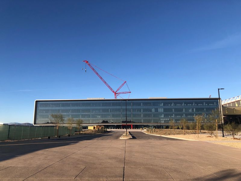
The below photo of the TSMC Arizona office building was taken in Q1 2023.

The below photo of the TSMC Arizona office building was taken in Q1 2023.
Intel Ohio Update:

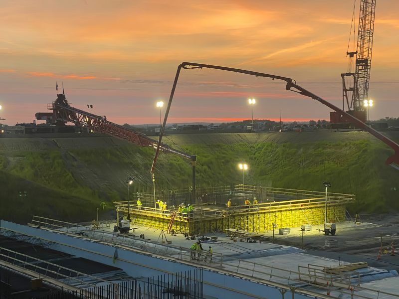
This week, Intel Corporation’s Ohio One construction teams began to pour more than 1,500 cubic yards of concrete, signaling our official shift into the next phase of #construction in the Silicon Heartland. I am very proud of our team and construction crew members for reaching this project milestone.
Our Ohio One site is reported to be the largest single private sector company investment in Ohio’s history — one that will create of tens of thousands of jobs across the state. This site is critical to our strategy to expand U.S. leading-edge semiconductor capabilities and develop a more resilient #semiconductor supply chain. As we begin setting the foundation for our future leading-edge factories, I want to thank our Intel team members, suppliers, partners, and the communities across the #BuckeyeState who are all involved in this project for making great progress on the site as we build a vibrant Intel future in Ohio. #IAmIntel #OhioOne #SiliconHeartland #Manufacturing
An interesting article that offers a binger picture of all these exciting activities in the semiconductor field: How real is America’s chipmaking renaissance? https://www.economist.com/business/2023/08/07/how-real-is-americas-chipmaking-renaissanceThree years ago, TSMC announced its intention to invest billions to build a fab in Arizona. Since then, we have announced our further commitment to bringing the most advanced semiconductor manufacturing to the U.S., including the announcement that TSMC Arizona’s first fab would produce N4 process technology by 2024 and the announcement that we have started the construction of a second fab that would produce 3nm process technology by 2026. Our total investment in Arizona is now $40 billion, making TSMC’s investment the largest foreign direct investment in Arizona history. Phase 1 is on track and on schedule to start production in late 2024 and we are currently in the process of moving-in and installing tools—including EUV tools, deposition systems, and wafer cleaning tools—into the fab. When operational, this will be the most advanced chip-manufacturing process technology on U.S. soil and our customers will benefit from having the proximity of a world-class foundry and the supply chain that surrounds this industry.
The below photo of the TSMC Arizona office building was taken in Q1 2023.
View attachment 1197
freshshine1
New member
Yep, here are the SemiWiki discussions for this articleAn interesting article that offers a binger picture of all these exciting activities in the semiconductor field: How real is America’s chipmaking renaissance? https://www.economist.com/business/2023/08/07/how-real-is-americas-chipmaking-renaissance
@nghanayem -
ascetic: a person who practices severe self-discipline and abstention.
I think the word you were looking for was
aesthetic: concerned with beauty or the appreciation of beauty.
ascetic: a person who practices severe self-discipline and abstention.
I think the word you were looking for was
aesthetic: concerned with beauty or the appreciation of beauty.

