Array
(
    [content] => 
    [params] => Array
        (
            [0] => /forum/index.php?threads/the-viability-of-fast-following.17273/page-2
        )

    [addOns] => Array
        (
            [DL6/MLTP] => 13
            [Hampel/TimeZoneDebug] => 1000070
            [SV/ChangePostDate] => 2010200
            [SemiWiki/Newsletter] => 1000010
            [SemiWiki/WPMenu] => 1000010
            [SemiWiki/XPressExtend] => 1000010
            [ThemeHouse/XLink] => 1000970
            [ThemeHouse/XPress] => 1010570
            [XF] => 2021370
            [XFI] => 1050270
        )

    [wordpress] => /var/www/html
)

The viability of fast following

N2 GAA is a yield learning node from what I understand so I don’t expect it to be used very much and not be around for long. We can expect the derivations of N2 I.E N2P, N2X to be appreciably more performant. N2 being conservative in its density improvements is consistent with TSMC’s regimented approach to nodes. Once they get GAA down I imagine what ever follows the base N2 will be quite competitive to 18A. Have you guys heard anything to the contrary?
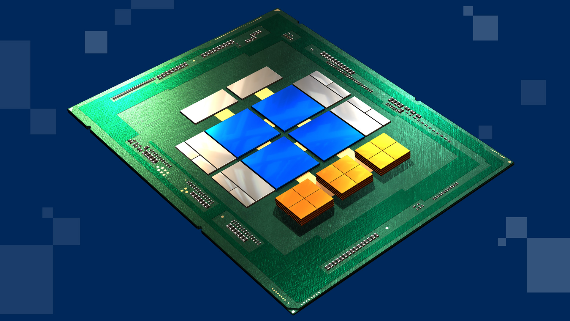
N2 is in a similar place to N16. People will either stay on N3 derivatives or wait for N1.4 (or whatever (N2)-1 is called). That doesn't necessarily mean that N2 will be short lived (N16 had a normal lifetime and was superceded on TSMC's normal cadence). By the time we get BSPD and maybe 4 HNSs with an N2X, it is totally feasible that 16A or 14A are on the market. Will these nodes be better than an N1.4? Nobody knows. What is known is that if 18A comes to market before N2 with a slight advantage. If this is the case then N1.4 better be a N7 moment rather than an 10FF moment. Also by your same logic isn't 20/18A also just a yield learning node. We know that M2P is not changing with 18A. A massive density jump will not be 20/18A's gig.

Not to say that TSMC needs to be in the lead (they don't), but it has let them pump up their margins. But if intel or Samsung (preferably both) can execute then if nothing else this will steal a minor amount of their share, and would force TSMC to lower their margins.
 
Last edited:
Why would Pat lose his job if his brainchild became the most successful part of the business? If anything wouldn't that put him on a Grove/Moore level of bailing on memory for CPUs? I assume I am misunderstanding your statement.
In the next sentence after the one you quoted, the "it" I was referring to was a trust transgression. I'm sorry for my clumsy grammar. I suppose the ultimate fears an IFS user might have, that the Intel design groups get a secretly diverted early test chip, or that an early die goes into an electron microscope, just seems profoundly unlikely. Nothing involving human behavior is impossible, but Intel is making a huge investment in fabs that could only be filled with IFS business. I just don't buy it.

And, yes, I also think that if IFS succeeds that Gelsinger will be at the same level as Grove in Intel culture.
 
A lot of the Intel investors I talk to are under the that impression once Intel gets even a marginal process lead then it will be off to races...
The question is whether it needs to beat TSMC, or just to beat Samsung, at least to be come viable and ready to divest as a true IFS. Sammy has a quite public culture of blame and secrecy, I wonder if Intel culture will get superior process control, solutions to problems, and yield? It seems like a business requiring a huge number of different competencies to work together in trust and collaboration to stay on track.
 
TSMC has been doing this convincingly for a decade, building more and more fabs, lowering their costs, acquiring more customers, lowering their costs more. Rinse and repeat.
It is not just volume. It is also customer diversity. TSMC does not have a big-leap and copy-exact style. It has an iterate-fabs with more of a Dutch-auction fill each fab with customers. It gets to see a broad perspective of needs and plan flexible coverage. Intel fabs for years had a semi-collaborative but captive model where there could be some negotiation of features but once it was decided, every chip had to fit and nothing other than the plan was going to have an ideal process. Even internally this was terribly difficult for mobile chips.

An IFS needs to be a customer oriented business, not a capture-the-customer business.
 
An IFS needs to be a customer oriented business, not a capture-the-customer business.
I think they know that. The question is, do they really know how to execute that strategy? I wonder if they've created an advisory group of their internal TSMC customers? If they haven't already, IFS needs to do this ASAP. They have numerous TSMC projects internally that can give them requirements and feedback.
 
I think they know that. The question is, do they really know how to execute that strategy? I wonder if they've created an advisory group of their internal TSMC customers? If they haven't already, IFS needs to do this ASAP. They have numerous TSMC projects internally that can give them requirements and feedback.

Will this type of activities trigger the legal, NDA, ethical, and integrity issues?

If such advisory group exists, it will kill the collobration between Intel and TSMC.
 
Will this type of activities trigger the legal, NDA, ethical, and integrity issues?

If such advisory group exists, it will kill the collobration between Intel and TSMC.
Asking internal groups that use foundries about their requirements is not unethical. The purpose of these advisors would not be to violate whatever non-disclosure agreements they've signed with TSMC. It would be find out how they operate with TSMC. What tools they need. What IP is important in their industries. How they use shuttles. (I assume that IFS, like GF and TSMC, will support shuttles.)

All design companies shop around and are courted by other fabs, like Samsung. Fabs have sales and marketing groups too. Having internal users of foundries will educate IFS about what they need. High level stuff like ecosystem partners and tools are public information anyway.

IFS is already committing $1B to fund companies participating in the IFS ecosystem.


IFS says a lot of good stuff on their design services webpages. I just wonder about how much this stuff is real and based on actual customer requirements.


"It would be find out how they operate with TSMC."

I'd be surprised if Intel hasn't built an internal firewall to prevent such "communication" or "learning" between Intel design division and Intel foundry service (IFS). Intel must enforce strict rules via the internal firewall.

Additionally, Intel is different from a fabless company, such as Qualcomm, Nvidia, and AMD. Remember IFS is a competitor of TSMC while Intel product division is a competitor of many IFS' potential customers.
 
Last edited:
Is IFS focused on 16nm, 22nm, and Tower (45, 65, 130, 180) processes?
Any predictions on what Intel's criteria will be for getting onto the MPW shuttles?
Will IFS be willing to package the MPW die onto an interposer with HBM within the next 2 years?
Should products with NRE budgets less than $10M stick to TSMC and GF?
Is IFS 22/16 for huge volume customers only?

Nothing is clear about IFS 1y+ after its supposed launch. I have yet to hear Intel itself coming forward, and explain out loud what they will do.

The first thing to tell about Intel near-leading edge is that they simply nowhere big enough throughput-wise in comparison to other 2nd tier fabs.

And Tower is too nowhere near even UMC.

40nm/45nm planar immersion, and 65 planar dry would've been a cash crop with current capacity crunch on legacy nodes, but again Tower been too niche, and too small to exploit that. Also, there are no IP on the market for their SOI process.
 
While I am not sure it was intentional, UMC often would be a fast follower to TSMC, and before 28nm this worked out well for them as designs could be easily ported from TSMC nodes to UMC nodes. Once TSMC started accelerating away and UMC's nodes stopped being design compatible this model fell apart, and UMC needed a more differentiated offering. Samsung and Intel are doubling down in an attempt to accelerate ahead of TSMC. The thought then crossed my mind if fast following could work for these IDMs. TSMC used fast following to great effect to accelerate past the other semiconductor companies with HKMG last, finFETs on bulk Si, and EUV. In the case of intel they are now benefiting from the work that TSMC and Samsung put in at 7 and 5nm to accelerate their own EUV efforts. With this I wonder if it would potentially be desirable to remain a fast follower rather than attempting to zoom ahead of the current technological leader?

To clarify I don't think these firms have any plans of doing this, given that Samsung has the ambitious goal to be the number one foundry and intel has the much more modest goal of being No.2. But I wonder if these firms chose a different path, or if their current path leads to a financial situations that makes "being in first place" becomes too expensive to justify. In theory it should be both easier to catch up to whomever is the current technological lead than to beat them due to all of the whitepapers, teardowns, and vendor experience acting as a strong tailwind. While this stopped working for UMC because their nodes stopped being plug and play with TSMC - giving TSMC an unassailable first movers advantage - but in theory the IDMs are not bound in a similar manner because their primary business is selling end product not wafers. In theory these IDMs don't have to have the best cost structure because they are selling the wafer at ASP*number working dies rather than wafer cost*1.X. Their captive customers also either can't leave or face significant capacity or cost penalties to leave (reducing the risk of a UMC situation). One additional benefit of this scheme could be that when new nodes are rolled out they could be in an even healthier state than a normal leading edge node would be when it is new, given the extra time it had to incubate (think things like UMC 14nm or GF 22/12 FDX which had to already be mature when they entered HVM).

In short; could staying at N+1 with TSMC be something that is sustained for a long period of time (with maybe a few outsourcing jobs or parts of an MCM design being thrown to TSMC here and there)? Or even with things like MCM and the general slowing of transistor improvements would the IDMs start bleeding share to competitors if they are always a bit behind on the process front (potentially risking that these IDMs even lose the scale needed to even "run the race" at a slower pace)? While it would certainly not be a way to build up a strong healthy foundry, would this business model allow the IDMs to "stay in the race" without having to burn mountains of cash and developing a foundry to help amortize their costs?

I think the lack of design portability after 40nm destroyed every chance for a next fast follower. TSMC itself played a fast follower extremely well, and managed to stay in the game until the bifurcation point to proprietary processes.

For the same reason, there is no opportunity left for any new legacy player to enter with something new, as the entire ecosystem been defined at the time when the node been leading edge. Nobody will be making new IP for "new legacy nodes."

I can only see a chance opening if 3-4 major 2nd tier fabs will unite, and share a what is called a "platform."

The term "platform" is what makes a common process, full set of EDA tools needed, cell libraries, 3rd party IP.

GF can do that with its 12FDX if it will somehow manage to get UMC to join. That is though highly unlikely given how ego driven both companies are.
I agree, hence why the UMC model fell apart. In theory IDMs don't have to worry about this ecosystem issue, and I was wondering if in a different timeline if Samsung or intel decided against foundry; if said IDMs can sustainability be in a fast follower position? Would this lower node development/ramp costs to the point that the economics make sense without foundry (or in the case of Samsung, a mega corporation and memory manufacturer to also prop up the IDM business)? Or would following this path make these IDMs eventually bleed enough wafers to either TSMC or fabless firms to bring these IDMs below the critical mass necessary to justify the expense?
 
Personally I think expectations were set too high after Pat Gelsinger joined Intel His "AMD is in the rear view mirror" comment said it all:

"All of a sudden, boom, we are back in the game. AMD in the rear view mirror in clients, and never again will they be in the windshield," Gelsinger says with a smile. “We are just leading the market." If you’re an Intel fan, you’ll love to hear the confidence. But if you’re team AMD, you’re likely rolling your eyes.

The same can be said about IFS. The foundry business is a marathon not a sprint. It really is a difficult business and not to be taken lightly. Under estimating TSMC is also a huge mistake as they are champion counter punchers. If you hit them once they will hit you back ten times.
I agree the Pat hype is .. a bit too high.

Though in some markets, AMD seems to need to have a node advantage to compete on a level playing field.

Desktop CPUs - 12th/13th gen are holding up just well against Zen 4 on N5 - both on price and outright performance.
Mobile CPUs - Intel was very competitive using the older 14nm and early “rough” 10nm processes competing against AMD’s mature N7 offerings.

Discrete GPUs (desktop and mobile) - 6000 series GPUs were still weaker than Nvidia’s offerings overall (though not by a lot) despite being on a much better TSMC N7 process (vs. Samsung’s 8N). Now with Nvidia on N4 and AMD on N5 for current gen, there’s a significant gap in perf/watt and total performance between AMD and Nvidia.

Basically if TSMC isn’t able to offer AMD a full node ahead of Intel, the rear view mirror claim may become correct. To do this, TSMC really needs to be ~ 1.5 nodes ahead of Intel since Apple is always using that first year of capacity on the newest node.
 
Desktop CPUs - 12th/13th gen are holding up just well against Zen 4 on N5 - both on price and outright performance.
Mobile CPUs - Intel was very competitive using the older 14nm and early “rough” 10nm processes competing against AMD’s mature N7 offerings.

Discrete GPUs (desktop and mobile) - 6000 series GPUs were still weaker than Nvidia’s offerings overall (though not by a lot) despite being on a much better TSMC N7 process (vs. Samsung’s 8N). Now with Nvidia on N4 and AMD on N5 for current gen, there’s a significant gap in perf/watt and total performance between AMD and Nvidia.
I think you are missing a couple of details here. AMD has better margins on intel indicating intel is selling closer to cost to be competitive (probably also helped by more of AMD's wafers going to server where AMD mostly stomps on intel). As for NVIDIA their products have much larger dies than AMD's.
 
Last edited:
I think you are missing a couple of details here. AMD has better margins on intel indicating intel is selling closer to cost to be competitive (probably also helped by more of their wafers going to server where AMD mostly stomps on intel). As for NVIDIA their products have much larger dies than AMD's.
Speaking of which i'd hope for Nvidia's sake they already are deep in development of chiplet designs because if they aren't they are going to have a big problem.
 
Speaking of which i'd hope for Nvidia's sake they already are deep in development of chiplet designs because if they aren't they are going to have a big problem.
Nvidia were early adopters for HBM and products like Grace-Hopper show they are working on efficient adjacent bus. So they will do their own calculations on what makes sense for their products and market. The GPUs have a high yield with big die due to redundancy.
 
I think you are missing a couple of details here. AMD has better margins on intel indicating intel is selling closer to cost to be competitive (probably also helped by more of AMD's wafers going to server where AMD mostly stomps on intel). As for NVIDIA their products have much larger dies than AMD's.
I agree I wasn’t considering margins there - and that’s totally fair. Do we have a good source or sources on the margins for Intel vs. AMD desktop and Mobile?.

Zen 3 was sorta brought to firesale prices by 12th gen, and Zen 4 doesn’t seem to be selling well relative to 12th gen or Zen 3… so prices are going to have to reduce there. I’d also expect N5 to be pricier per mm2 than Intel 7 at this point..

(As a quick comparator - 13700K/13900K have 257mm2 dies, 7900X/7950X are 140mm2 (2x70, on N5) + a 122mm2 I/O die for 262mm2 of die sizes, with 140mm2 of that on a relatively expensive process (though easier to yield smaller dies)).

For Nvidia vs. AMD GPUs - Nvidia definitely had larger dies but on a process that should be substantially cheaper per mm2 - Samsung N8 vs TSMC N7. That’s previous gen. On current gen, Nvidia’s 4080 is roughly equal to 7900XTX (a little slower on Raster, but much faster on Raytracing) with a 379mm2 vs 520mm2 die. Nodes are “comparable” - TSMC N5 vs TSMC N4.

Lastly, Nvidia and Intel have higher volume (4-5x?) which should help with costs somewhat..

It’s just a gut feel that AMD needs some sort of manufacturing tech edge to “win” against these two — whether it’s stacked cache to tie/win on games, or a more advanced manufacturing node, or both.
 
I agree I wasn’t considering margins there - and that’s totally fair. Do we have a good source or sources on the margins for Intel vs. AMD desktop and Mobile?.

Zen 3 was sorta brought to firesale prices by 12th gen, and Zen 4 doesn’t seem to be selling well relative to 12th gen or Zen 3… so prices are going to have to reduce there. I’d also expect N5 to be pricier per mm2 than Intel 7 at this point..

(As a quick comparator - 13700K/13900K have 257mm2 dies, 7900X/7950X are 140mm2 (2x70, on N5) + a 122mm2 I/O die for 262mm2 of die sizes, with 140mm2 of that on a relatively expensive process (though easier to yield smaller dies)).
I don't have hard evidence to support this, but given i7 has a higher mask count than i4 (similar pitches to N5) I would assume that N5 is at worst similar in price. Even at that same price you are also getting far more transistors than i7 per mm^2. Obviously AMD needs to pay like a 50-60% mark up whereas foundry is giving the wafer away. But you get the idea.
 
In theory it should be both easier to catch up to whomever is the current technological lead than to beat them due to all of the whitepapers, teardowns, and vendor experience acting as a strong tailwind.
Seems practical to me. If the "fast follower" provides MPW shuttles and good packaging options, I am sure they will do quite well.
I think the lack of design portability after 40nm destroyed every chance for a next fast follower. TSMC itself played a fast follower extremely well, and managed to stay in the game until the bifurcation point to proprietary processes.
I don't understand "lack of portability". Do you expect push button migrations? Is that what Intel does? For the RTL, don't they resynthesize, P&R, and adjust timing?

For analog, if the circuit designer saves their testbenches and takes good notes, etc, what is problem sliding over? The design is going to change anyway, because designs improve. More testability, calibration, etc. What was minimum before goes to the new minimum. Things not at minimum will probably get retuned. Use the same testbenches. The problem with migrations is typically due to not packaging up the design properly at the end of the project. The PM needs to be tarred and feathered.

Please explain what make the move so scary. 40 => 28... maybe not worth it. 40=>16... may be worth it.
 
Back
Top