SRAM cell asymptotic scaling can be traced to CPP scaling hitting a wall somewhere above 40 nm.
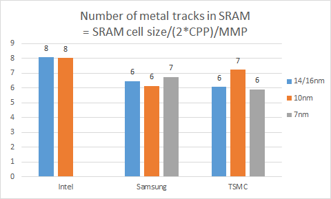
First, it is established (in the inset) that the SRAM cell is basically (2*contacted poly pitch) x (# of minimum metal pitch), where the # is shown to be around 6 for Samsung and TSMC and 8 for Intel.

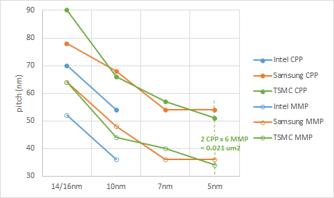
Then we can project the range of 5nm pitches for TSMC based on 0.021 um2 SRAM cell size.

The expected range of CPP indicates an asymptotic flattening, heading from 7nm to 5nm. This asymptotic limit is well above the MMP level, so it is not based on patterning, but due to the short channel effects like DIBL and SS degradation. Also, note that Samsung's 5nm pitches are already announced to be flat with 7nm.
First, it is established (in the inset) that the SRAM cell is basically (2*contacted poly pitch) x (# of minimum metal pitch), where the # is shown to be around 6 for Samsung and TSMC and 8 for Intel.
Then we can project the range of 5nm pitches for TSMC based on 0.021 um2 SRAM cell size.
The expected range of CPP indicates an asymptotic flattening, heading from 7nm to 5nm. This asymptotic limit is well above the MMP level, so it is not based on patterning, but due to the short channel effects like DIBL and SS degradation. Also, note that Samsung's 5nm pitches are already announced to be flat with 7nm.

