Interesting. Do the slides have a date? Was it before 6nm was officially announced (May 2019) ? TSMC 7+ is obsolete now that TSMC 6nm is in play. I'm not sure why AMD would put the effort into 7+ for a small density increase when they can do 5nm or easily migrate 7nm designs to 6nm. I also met with Nvidia and they are still on TSMC 7nm and will migrate to 6nm.
I would really be surprised if AMD and Nvidia do NOT split manufacturing between TSMC and Samsung. Two foundry sources is always better than one and margins are everything for fabless chip companies.
It will be interesting to see what happens at SEMICON West next month. Scott Jones and I will be there and the meeting requests just keep on coming. Intel hired some outsiders for marketing so there are a lot of familiar faces this year.
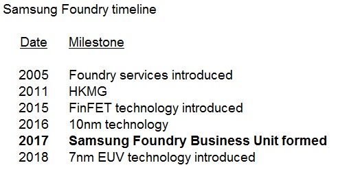
Daniel TSMC 7+ is already in volume production while N6 will start risk production in Q1 2020, be ready for tapeouts in H2 2020 and volume production is slated for end of 2020. TSMC stated in their earnings call that a few of their customers have taped out on 7+ this year. AMD's Zen 3 is stated to have taped out (from a friend of mine who has sources at AMD) on TSMC 7+ in late Jan 2019. AMD's roadmap also states 7nm+ Zen 3 in 2020. Moreover I think N7+ will have the best PPA compared to the other versions. TSMC has 4 process versions.
1. TSMC N7 DUV (in volume production from Q2 2018) - 1st gen 7nm DUV
2. TSMC N7P DUV (in volume production from Q2 2019) aka 2nd gen 7nm DUV - fully design rule compatible with 1st gen 7nm DUV . >= +5% transistor perf at same power vs N7 DUV
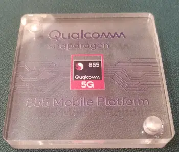
TSMC 7nm HD and HP Cells, 2nd Gen 7nm, And The Snapdragon 855 DTCO
Update and analysis of TSMC 7-nanometer node low-power and high-performance cells, 2nd generation 7nm, and the design technology co-optimization (DTCO) effort that went into the Snapdragon 855 SoC.
3. TSMC N6 EUV (risk production Q1 2020 and volume production end of 2020) - design rule compatible with 1st gen 7nm DUV. If you want the area shrink you have to retapeout (RTO) the N7 DUV design.
4. TSMC N7+ EUV (in volume production from Q2 2019) . I think this is the highest performing 7nm process from TSMC with the best feature set and will be used by companies who require the highest transistor performance.
TSMC Technologies for Mobile and HPC - Semiwiki
During TSMC 2018 Technology Symposium, Dr. B.J. Woo, TSMC VP of Business Development presented market trends in the area of mobile applications and HPC computing as well as shared TSMC progress in making breakthrough efforts in the technology offerings to serve these two market segments. Both 5G...
The N7+ value proposition includes delivering 20% more logic density over N7, 10% lower power at same speed, and additional performance improvements anticipated from the ongoing collaboration with customers .
TSMC's 7nm+ EUV is in production, improves performance by 10%
Despite how young 7nm technologies are, having yet to appear in a single laptop or desktop, they are already superseded by 7nm+.
At TSMC’s recent technology forum in Hsinchu, Taiwan, the company's CEO confirmed new details regarding N7+, TSMC’s refined 7nm node employing EUV (extreme ultraviolet) lithography. Most importantly, N7+ chips are already being produced and 7nm production will ramp up by 150% this year to one million total units.
7+ has identical yield rates to N7 and will steadily improve, while also offering a 20% increase to transistor density. There’s also a 10% performance uplift or 15% power efficiency increase.
As for Nvidia using TSMC and Samsung at 7nm they have officially confirmed it.
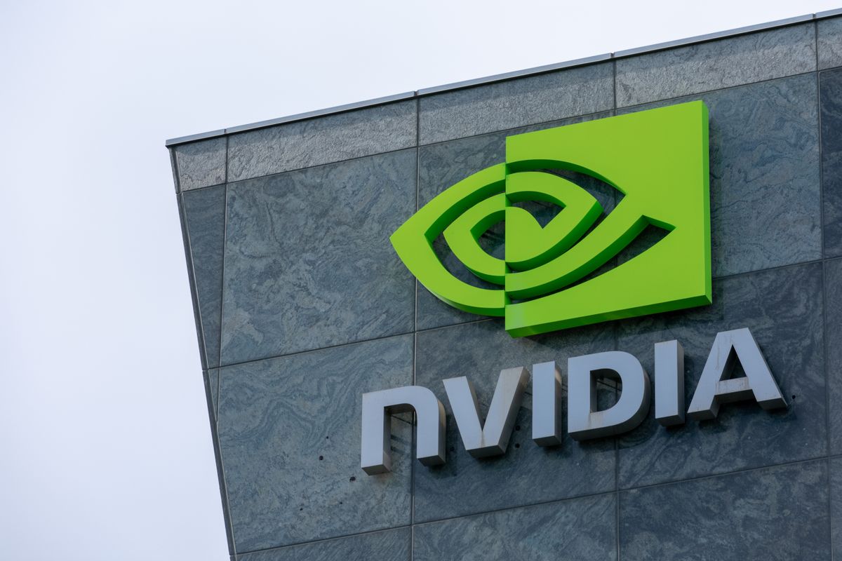
Update: Nvidia VP Says Next-Gen GPUs Will Be Made by TSMC and Samsung
Nvidia reportedly confirmed that it's partnered with Samsung to manufacture its Ampere GPU, which is expected to launch in 2020 using its 7nm EUVL process.
Nvidia executive vice president of operations Debora Shoquist said in a statement that “Recent reports are incorrect – NVIDIA’s next-generation GPU will continue to be produced at TSMC. NVIDIA already uses both TSMC and Samsung for manufacturing, and we plan to use both foundries for our next-generation GPU products.
AMD on the other hand is completely on TSMC 7nm and has confirmed the same. Unless AMD face supply constraints they are likely to stick with TSMC 7nm across their product lineup.
_678x452.jpg)