2020/08/20
Lipen Yuan, Director, Advanced Technology Business Development, TSMC
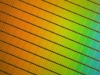
TSMC marked an amazing milestone in the past month of July – we manufactured our one-billionth good die on our 7-nanometer (7nm) technology; in layman’s terms, that would be one billion functional, defect-free 7nm chips.

A remarkable achievement for a technology that entered volume production in April 2018. Since then, we have manufactured 7nm chips for well over 100 products from dozens of customers. It is enough silicon to cover more than 13 Manhattan city blocks, and with more than a billion transistors per chip, this is true Exa level, or over one quintillion 7nm transistors.
TSMC’s large-scale, efficient manufacturing means more than just producing a lot of chips quickly. It is critical to improving quality and reliability, and the learning enables technology advancement.
Practice Makes Perfect
Our 7nm technology ramped to high-volume production faster than any other TSMC technology before. As with any skill, practice makes perfect in chip manufacturing. The more chips you make, the more you learn - where defects can occur, or where new materials or equipment cause unexpected results, and the more opportunity you have to learn how to eliminate these problems and optimize the process. As the first foundry to bring 7nm technology into high-volume production, TSMC has had more time and wafers to improve our quality and yield more than any other semiconductor manufacturer. TSMC has deployed extensive sensors in our equipment to ensure that every piece of useful data is collected, and we use artificial intelligence and machine learning to turn that data into knowledge and intelligence to improve our manufacturing. Not one opportunity to learn goes to waste.
Good quality and reliability do not just lead to satisfied customers, it can also open up markets and new opportunities. Our Automotive customers have always asked for the highest level of quality, because safety is their number one concern. They are now also asking for advanced technology to support the sophisticated computing needed for Advanced Driver Assistance Systems (ADAS) and autonomous driving. These two demands are not easy to balance – advanced technology is always new, by its nature, but achieving automotive-grade quality takes time and experience. Thanks to the experience and learning built up from the scale of our 7nm manufacturing, we were able to work with our colleagues in Quality and Reliability to deploy our stringent Automotive Quality System to the 7nm process in 2019. That successfully put our most advanced technology at the time into the hands of our automotive customers.
A Solid Foundation for Innovation
The experience and learning that comes from high-volume manufacturing can go beyond fixing problems and enhancing quality; they also push the technology forward. During the 7nm generation, TSMC introduced the long-anticipated extreme ultraviolet (EUV) lithography, a technology that the industry had been looking forward to for many years. The smaller wavelength of EUV light allows us to print the nanometer-scale features of advanced technology designs more easily. At the same time, EUV light is much more difficult to create – it requires hitting tiny droplets of tin with pulses from a powerful source laser to turn the droplets into a plasma, which then emits the wavelength of light we desire. As the first company to bring EUV into commercial production at the 7nm generation, our accumulated experience allowed us to lead the semiconductor industry once again this year with volume production of 5nm technology, which is our most advanced process today.
The success of our 7nm process has not stopped us from continued innovation in this family of technologies. We have extended our 7nm technology in to a new family member, our N6 process. N6 is in volume production today, using EUV to replace conventional immersion layers. TSMC’s N6 offers a new standard cell with nearly 20% logic density improvement. Its design rules are completely compatible with its N7 predecessor, and delivers an excellent cost-effective option for our customers’ next wave of 7nm generation designs.
Thriving Demand for Advanced Technology
The launch of our 7nm technology was a big moment for TSMC. It marked the first time in history that the most advanced logic technology, as an open platform, was available for all the designers in the semiconductor industry. Today, one billion good dies later, we can see that designers of chips for all types of different applications are very eager to get their hands on the most advanced technology.
This was not always the case. In the past, only a limited number of applications asked for the horsepower offered by leading-edge technology, applications such as PC processors, graphics processors, and FPGAs. The introduction of the smartphone opened up more demand, putting leading-edge chips into the pockets of hundreds of millions of consumers, but now with the rise of cloud computing and artificial intelligence, there are more applications than ever. TSMC’s 7nm technology is not only in PCs, tablets, and smartphones, they are in data centers, in automobiles, and performing sophisticated training and inferencing for AI. With the deployment of 5G infrastructure creating stable networks for quickly sending large volumes of data, the demand for leading-edge chips to process this data will only become greater. I look forward to seeing the new applications that innovators will create.
So for TSMC, that is the meaning of one billion good dies: it represents the refinement of our craft, a foundation for innovation, and a healthy, thriving demand for advanced technology. We anticipate more exciting innovations to come.
 www.tsmc.com

Lipen Yuan, Director, Advanced Technology Business Development, TSMC
TSMC marked an amazing milestone in the past month of July – we manufactured our one-billionth good die on our 7-nanometer (7nm) technology; in layman’s terms, that would be one billion functional, defect-free 7nm chips.
A remarkable achievement for a technology that entered volume production in April 2018. Since then, we have manufactured 7nm chips for well over 100 products from dozens of customers. It is enough silicon to cover more than 13 Manhattan city blocks, and with more than a billion transistors per chip, this is true Exa level, or over one quintillion 7nm transistors.
TSMC’s large-scale, efficient manufacturing means more than just producing a lot of chips quickly. It is critical to improving quality and reliability, and the learning enables technology advancement.
Practice Makes Perfect
Our 7nm technology ramped to high-volume production faster than any other TSMC technology before. As with any skill, practice makes perfect in chip manufacturing. The more chips you make, the more you learn - where defects can occur, or where new materials or equipment cause unexpected results, and the more opportunity you have to learn how to eliminate these problems and optimize the process. As the first foundry to bring 7nm technology into high-volume production, TSMC has had more time and wafers to improve our quality and yield more than any other semiconductor manufacturer. TSMC has deployed extensive sensors in our equipment to ensure that every piece of useful data is collected, and we use artificial intelligence and machine learning to turn that data into knowledge and intelligence to improve our manufacturing. Not one opportunity to learn goes to waste.
Good quality and reliability do not just lead to satisfied customers, it can also open up markets and new opportunities. Our Automotive customers have always asked for the highest level of quality, because safety is their number one concern. They are now also asking for advanced technology to support the sophisticated computing needed for Advanced Driver Assistance Systems (ADAS) and autonomous driving. These two demands are not easy to balance – advanced technology is always new, by its nature, but achieving automotive-grade quality takes time and experience. Thanks to the experience and learning built up from the scale of our 7nm manufacturing, we were able to work with our colleagues in Quality and Reliability to deploy our stringent Automotive Quality System to the 7nm process in 2019. That successfully put our most advanced technology at the time into the hands of our automotive customers.
A Solid Foundation for Innovation
The experience and learning that comes from high-volume manufacturing can go beyond fixing problems and enhancing quality; they also push the technology forward. During the 7nm generation, TSMC introduced the long-anticipated extreme ultraviolet (EUV) lithography, a technology that the industry had been looking forward to for many years. The smaller wavelength of EUV light allows us to print the nanometer-scale features of advanced technology designs more easily. At the same time, EUV light is much more difficult to create – it requires hitting tiny droplets of tin with pulses from a powerful source laser to turn the droplets into a plasma, which then emits the wavelength of light we desire. As the first company to bring EUV into commercial production at the 7nm generation, our accumulated experience allowed us to lead the semiconductor industry once again this year with volume production of 5nm technology, which is our most advanced process today.
The success of our 7nm process has not stopped us from continued innovation in this family of technologies. We have extended our 7nm technology in to a new family member, our N6 process. N6 is in volume production today, using EUV to replace conventional immersion layers. TSMC’s N6 offers a new standard cell with nearly 20% logic density improvement. Its design rules are completely compatible with its N7 predecessor, and delivers an excellent cost-effective option for our customers’ next wave of 7nm generation designs.
Thriving Demand for Advanced Technology
The launch of our 7nm technology was a big moment for TSMC. It marked the first time in history that the most advanced logic technology, as an open platform, was available for all the designers in the semiconductor industry. Today, one billion good dies later, we can see that designers of chips for all types of different applications are very eager to get their hands on the most advanced technology.
This was not always the case. In the past, only a limited number of applications asked for the horsepower offered by leading-edge technology, applications such as PC processors, graphics processors, and FPGAs. The introduction of the smartphone opened up more demand, putting leading-edge chips into the pockets of hundreds of millions of consumers, but now with the rise of cloud computing and artificial intelligence, there are more applications than ever. TSMC’s 7nm technology is not only in PCs, tablets, and smartphones, they are in data centers, in automobiles, and performing sophisticated training and inferencing for AI. With the deployment of 5G infrastructure creating stable networks for quickly sending large volumes of data, the demand for leading-edge chips to process this data will only become greater. I look forward to seeing the new applications that innovators will create.
So for TSMC, that is the meaning of one billion good dies: it represents the refinement of our craft, a foundation for innovation, and a healthy, thriving demand for advanced technology. We anticipate more exciting innovations to come.
Celebrating One Billion 7nm Chips: Why Scale Matters - Taiwan Semiconductor Manufacturing Company Limited
TSMC marked an amazing milestone in the past month of July – we manufactured our one-billionth good die on our 7-nanometer (7nm) technology; in layman’s terms, that would be one billion functional, defect-free 7nm chips.
www.tsmc.com
Last edited: