You are currently viewing SemiWiki as a guest which gives you limited access to the site. To view blog comments and experience other SemiWiki features you must be a registered member. Registration is fast, simple, and absolutely free so please, join our community today!
It looks like chiplet technologies are going to be the next area of fierce competition. Who do the SemiWiki community feels will win this contest and where is chiplet technology going. Will this be the dominant technology of the future or just one of many options? Who will be the winners in providing materials, equipment and EDA for this area? Also appreciated would be the timeline for these changes to take place and the percentage of the market that chiplets and related technology to take hold? Thanks
It comes down to SIP packaging cost. Radio Shack days be gone! Focus on performance, power, and NRE costs. Too much emphasis in the forum on saving pennies on die costs IMO. I mean no disrespect. The technologist on this website are awesome, but believe it's all about lowering NRE and reducing design cycle time of the system, not die costs. If your die is 25% bigger, who cares? Make the system and reduce your time to market. Get out of the commodity business.
Circuit designers must construct the system of multiple chips with a bunch of wires (BOW). Chiplets flipchipped onto interposer at a pitch of 55-40um. HBM3 standard seems to be 40um pitch. MPWs are at 150-110um pitch. TSMC documents publicly for a 55um pitch bumps for die mounting onto an interposer. I don't know what the other foundries are pushing. Amkor referred me to foundries when I asked about pad pitches below 90nm. Perhaps one of the many knowledgeable process people on this site can comment on the difficulty of having old technology fabs (0.5u ok) focus on interposers, with perhaps through silicon vias. They will supply your answer.
Is Skywater the only old technology foundry to figure out the importance of interposers?
On the flip side, big SOCs will melt and have yield issues. That giant Apple chip is ridiculous.
It comes down to SIP packaging cost. Radio Shack days be gone! Focus on performance, power, and NRE costs. Too much emphasis in the forum on saving pennies on die costs IMO. I mean no disrespect. The technologist on this website are awesome, but believe it's all about lowering NRE and reducing design cycle time of the system, not die costs. If your die is 25% bigger, who cares? Make the system and reduce your time to market. Get out of the commodity business.
Circuit designers must construct the system of multiple chips with a bunch of wires (BOW). Chiplets flipchipped onto interposer at a pitch of 55-40um. HBM3 standard seems to be 40um pitch. MPWs are at 150-110um pitch. TSMC documents publicly for a 55um pitch bumps for die mounting onto an interposer. I don't know what the other foundries are pushing. Amkor referred me to foundries when I asked about pad pitches below 90nm. Perhaps one of the many knowledgeable process people on this site can comment on the difficulty of having old technology fabs (2u ok) focus on interposers, with perhaps through silicon vias. They will supply your answer.
Is Skywater the only old technology foundry to figure out the importance of interposers?
On the flip side, big SOCs will melt and have yield issues. That giant Apple chip is ridiculous.
Is it my understanding the cost and yield benefits of chiplets is really a secondary benefit and not the primary reason they are the used. Chiplets enabled disaggregated dies which allowed the offloading of the worst scaling parts of compute elsewhere on the substrate so you can focus the limited compute real estate on logic and not the ever increasing cache allocations. Interconnects will never be as fast a monolithic die but the compute space and design modularity chiplets provide more then makes up for relative interconnect latency penalties . This is all my understanding so I’d appreciate being corrected if I’m off base here.
The interconnect for an HBM3 (high bandwidth memory) is crazy fast. It handles 1024 parallel inputs 6.4GHz on tiny wires. 64bits * 16 channels. A 5sqmm chiplet can connect to that HBM directly. No current mode logic (50 ohm terminations). No need to put an enormous amount of SRAM on the expensive main chip. The interposer is also a piece of silicon. Just make sure the metal is thin enough so that it is all skin. Keep that RC low. I forgot to calculate that in a previous comment. The cost of the interposer is probably astronomically high presently. Give it 3 years?
It's possible that the exotic memory changes that game again and makes the big SOC more feasible. The strategy changes monthly with technology changes and geopolitics. My predictions expire in 30 days.
Is it my understanding the cost and yield benefits of chiplets is really a secondary benefit and not the primary reason they are the used. Chiplets enabled disaggregated dies which allowed the offloading of the worst scaling parts of compute elsewhere on the substrate so you can focus the limited compute real estate on logic and not the ever increasing cache allocations. Interconnects will never be as fast a monolithic die but the compute space and design modularity chiplets provide more then makes up for relative interconnect latency penalties . This is all my understanding so I’d appreciate being corrected if I’m off base here.
I think time-to-market is a big benefit of chiplets. Just like commercial IP, using silicon proven IP blocks or die reduces risk and saves time. The commercial IP market outgrows semiconductor an EDA every year. Chiplets may do the same. As long as the foundries back chiplets, like they do commercial IP, and provide an ecosystem, chiplets will play an important role in semiconductor design, absolutely.
It looks like chiplet technologies are going to be the next area of fierce competition. Who do the SemiWiki community feels will win this contest and where is chiplet technology going. Will this be the dominant technology of the future or just one of many options? Who will be the winners in providing materials, equipment and EDA for this area? Also appreciated would be the timeline for these changes to take place and the percentage of the market that chiplets and related technology to take hold? Thanks
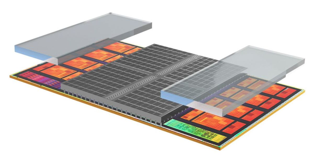
IMO, you're asking the wrong questions. Materials and equipment are not the primary factors in determining winners, though EDA will play an important role. (EDA always does.) The big wins from chiplets are reducing large die sizes, and enabling 3D chiplet stacking. Stacking, properly designed for and implemented, can be a huge advantage for high-performance chip design. The questions are also which design problems can best leverage architectures that can best take advantage of chiplets. Chiplets can cause performance issues versus monolithic dies, unless the partitioning strategy is focused on chiplet-specific issues. You don't just partition a big die and turn it into a chiplet design. Some companies, Nvidia comes to mind, are avoiding chiplets and stick to huge dies because they want the best performance even if it means higher costs. Cerebras, with its unique wafer-scale processor, is even farther afield from chiplets. The most significant companies I'm aware of which are pursuing chiplets include AMD for CPUs (AMD was really a pioneer), Intel (CPUs and Ethernet switches, and the primary contributor of the UCIe specification for inter-chiplet communications), and Broadcom (Ethernet switches). Ethernet switches appear to be an almost ideal case for realizing the value of chiplets, due to huge monolithic die sizes and the need for integrated transceivers and optics. I suspect Intel trailed AMD into chiplets for CPUs because Intel's CPU design team was reluctant to rip their CPU chip architecture apart, and Intel's fabs said they could name the massive die size yield problem tune in fewer notes than they could actually achieve.
IMO, designing for chiplets is still in its very early stages. I think it'll take multiple generations for design teams to get really good it, and for a rich chiplet support ecosystem to emerge.
Ding 1: Is Intel's floorplanning difficulties be due to being digital on top? If top level schematic and layout are in analog mode, the partitioning should be business as usual, except for the pain of dealing with the bumps and the ESDs. Am I wrong in saying that Intel relies too much on automation and static timing? Shouldn't blocks be gated, and sometime go through a synchronizer? Maybe Intel should employ an analog guy that also handles PLLs, and a good top level layout designer? Will it take Intel 2 generations... probably, because when you are a hammer, everything looks like a nail. Disclosure: I am analog and biased.
Ding 2: "Intel's CPU design team was reluctant to rip their CPU chip architecture apart". Are you kidding me? You digital guys are not supposed to be stick-in-the-muds. That role is reserved for analog designers. Shameful! Is that why Jim Keller left?
Ding 2: "Intel's CPU design team was reluctant to rip their CPU chip architecture apart". Are you kidding me? You digital guys are not supposed to be stick-in-the-muds. That role is reserved for analog designers. Shameful! Is that why Jim Keller left?
I thought the rumor was that he left due to intel not wanting to outsource as hard as he wanted? Although that rumor seems odd to me, given intel can't really outsource anymore than it is without literally stopping all R&D efforts. If this is true though then I highly disagree with him (not that I'd imagine he cares what a recent collage grad thinks). Disclosure: I am a process engineer and biased
Shouldn't blocks be gated, and sometime go through a synchronizer? Maybe Intel should employ an analog guy that also handles PLLs, and a good top level layout designer? Will it take Intel 2 generations... probably, because when you are a hammer, everything looks like a nail. Disclosure: I am analog and biased.
Just FYI, mostly for non-experts, an interesting non-technical article from IEEE Spectrum regarding 3D chiplets, and the web page includes several links to other interesting articles.
Our ability to shrink transistors and the logic and memory blocks they make up is slowing down. Plus, chips have reached their size limits. Photolithography tools can only pattern an area of about 850 square millimeters, about the size of a top Nvidia GPU. This is why the industry is now looking up.
Would apple's M1 SoCs count as chiplets? They don't use an interposer but it seems like they get a decent chunk of the performance advantages by locating main memory right beside the die.
Would apple's M1 SoCs count as chiplets? They don't use an interposer but it seems like they get a decent chunk of the performance advantages by locating main memory right beside the die.
I think of the M-series CPUs as "system in package", SiP chips. The term chiplet is normally used to designate a die that functions with other dies to give the appearance at the system level of a single chip. Too much ambiguity for me and a lot of folks, so I actually like Intel's tiled die terminology better, because it doesn't make insinuations about functionality.
I think of the M-series CPUs as "system in package", SiP chips. The term chiplet is normally used to designate a die that functions with other dies to give the appearance at the system level of a single chip. Too much ambiguity for me and a lot of folks, so I actually like Intel's tiled die terminology better, because it doesn't make insinuations about functionality.
What you're discussing is currently only true for the M1 Ultra, which is really two M1 MAX single die CPUs with a silicon interposer between them, so an Ultra really functions like an enormous single die CPU. The rest of the M1 and M2 CPUs are single dies in an SiP design.
What you're discussing is currently only true for the M1 Ultra, which is really two M1 MAX single die CPUs with a silicon interposer between them, so an Ultra really functions like an enormous single die CPU. The rest of the M1 and M2 CPUs are single dies in an SiP design.
The Apple CPU designs don't employ chiplets by the definitions other companies, like AMD, are using. The memory chips in the M1/M2 are connected with standard DDR5 interfaces.