Hardest hit are ≤200mm wafer fabs, 70% of closures in Japan and North America.
Over the past decade, the IC industry has been paring down its older capacity as manufacturers have consolidated or transitioned to the fab-lite or fabless business models. In its recently released Global Wafer Capacity 2020-2024 report, IC Insights shows that due to the surge of merger and acquisition activity in the middle of this decade and with more companies producing IC devices using sub-20nm process technology, suppliers have eliminated inefficient wafer fabs. Since 2009, semiconductor manufacturers around the world have closed or repurposed 100 wafer fabs, according to findings in the new report.
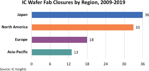
Figure 1 shows the number of fabs closed by geographic region while Figure 2 shows a distribution of those fabs by wafer size and year.

Figure 1
Japan and North America, have accounted for most of the wafer fab closures since 2009. Many of the shuttered wafer fabs had been used for decades and had outlived their useful purpose. Consequently, these fabs were closed in favor of much more cost-efficient facilities. In some cases, the cost of fab ownership became too great of a burden and several companies opted for the fab-lite or fabless business model that outsources manufacturing to a wafer foundry.

Figure 2
IC Insights has identified four additional wafer fabs—one owned by NJR, two at Renesas, and one operated by Analog Devices—that are slated to close in the 2020-21 timeperiod. Given the skyrocketing cost of new wafer fabs and manufacturing equipment, and as more IC companies transition to a fab-lite or fabless business model, IC Insights anticipates there will be more fab closures in the next few years. Fortunately, much of the “dead wood” (old fabs) has already been cleared out and the global manufacturing capacity that remains is regarded as fairly efficient.
It is worth noting, however, that a wave of fab closures came shortly after the Great Recession of 2007-2008 when companies were closely scrutinizing their operating costs. A decade later and with the Covid-19 virus wreaking havoc on global businesses and greatly impacting the global economy, could another wave of fab closures be in store?
Report Details: Global Wafer Capacity 2020-2024
IC Insights’ Global Wafer Capacity 2020-2024—Detailed Analysis and Forecast of the IC Industry’s Wafer Fab Capacity report assesses the IC industry’s capacity by wafer size, minimum process geometry, technology type, geographic region, and device type through 2024. The report includes detailed profiles of the companies with the greatest fab capacity and gives comprehensive specifications on existing wafer fab facilities. Global Wafer Capacity 2020-2024 is priced at $4,890 for an individual user license. A multi-user worldwide corporate license is available for $7,590.
PDF Version of This Bulletin
A PDF version of this Research Bulletin can be downloaded from our website at http://www.icinsights.com/news/bulletins/
Over the past decade, the IC industry has been paring down its older capacity as manufacturers have consolidated or transitioned to the fab-lite or fabless business models. In its recently released Global Wafer Capacity 2020-2024 report, IC Insights shows that due to the surge of merger and acquisition activity in the middle of this decade and with more companies producing IC devices using sub-20nm process technology, suppliers have eliminated inefficient wafer fabs. Since 2009, semiconductor manufacturers around the world have closed or repurposed 100 wafer fabs, according to findings in the new report.
Figure 1 shows the number of fabs closed by geographic region while Figure 2 shows a distribution of those fabs by wafer size and year.
Figure 1
Japan and North America, have accounted for most of the wafer fab closures since 2009. Many of the shuttered wafer fabs had been used for decades and had outlived their useful purpose. Consequently, these fabs were closed in favor of much more cost-efficient facilities. In some cases, the cost of fab ownership became too great of a burden and several companies opted for the fab-lite or fabless business model that outsources manufacturing to a wafer foundry.

Figure 2
IC Insights has identified four additional wafer fabs—one owned by NJR, two at Renesas, and one operated by Analog Devices—that are slated to close in the 2020-21 timeperiod. Given the skyrocketing cost of new wafer fabs and manufacturing equipment, and as more IC companies transition to a fab-lite or fabless business model, IC Insights anticipates there will be more fab closures in the next few years. Fortunately, much of the “dead wood” (old fabs) has already been cleared out and the global manufacturing capacity that remains is regarded as fairly efficient.
It is worth noting, however, that a wave of fab closures came shortly after the Great Recession of 2007-2008 when companies were closely scrutinizing their operating costs. A decade later and with the Covid-19 virus wreaking havoc on global businesses and greatly impacting the global economy, could another wave of fab closures be in store?
Report Details: Global Wafer Capacity 2020-2024
IC Insights’ Global Wafer Capacity 2020-2024—Detailed Analysis and Forecast of the IC Industry’s Wafer Fab Capacity report assesses the IC industry’s capacity by wafer size, minimum process geometry, technology type, geographic region, and device type through 2024. The report includes detailed profiles of the companies with the greatest fab capacity and gives comprehensive specifications on existing wafer fab facilities. Global Wafer Capacity 2020-2024 is priced at $4,890 for an individual user license. A multi-user worldwide corporate license is available for $7,590.
PDF Version of This Bulletin
A PDF version of this Research Bulletin can be downloaded from our website at http://www.icinsights.com/news/bulletins/

