
- This event has passed.
Locate and Solve ESD Design Challenges and Analyze Parasitic Networks Webinar
June 25, 2020 @ 10:00 AM - 11:00 AM
FREE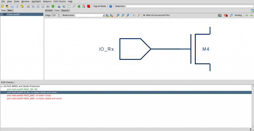
Overview:
As geometries of integrated circuits get smaller and complex, electrostatic discharge (ESD) and Parasitic related design issues become prevalent.
In this webinar we will show you a few methodologies to help reduce the design cycle by identifying ESD protection schemes in your netlist and assist in the verification of the point-to-point parasitic resistance between pads and the ESD devices. Sign up Today
What you will learn:
- How to identify missing ESD protection schemes quickly at the netlist level
- Save on simulation time by identifying ESD issues statically.
- Custom program your own ESD rules via Tcl
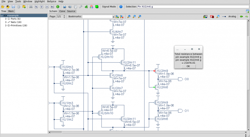
- Visualize and Analyze parasitic (RC) networks
- Calculate pin to pin resistance
Who should attend:
- Mixed Signal Design and Verification Engineers / Managers
- ESD Engineers
- IC Analog Engineers
- IC CAD Engineers


The Data Crisis is Unfolding – Are We Ready?